
Executive Summary
This industry report analyzes the critical application of plastic sheet vacuum thermoforming in electronic packaging, emphasizing the paramount importance of robust anti-static properties for protecting sensitive electronic components. As electronics become increasingly miniaturized and complex, packaging requirements demand higher ESD (Electrostatic Discharge) protection. Traditional surface anti-static coatings, limited by their temporary nature and susceptibility to wear, are often inadequate for advanced electronics. In contrast, permanent built-in ESD technologies offer lasting performance, consistent reliability, and comprehensive protection, establishing a new industry standard. This report provides a comparative analysis, case studies, and strategic insights to guide electronics manufacturers in adopting these superior packaging solutions, thereby enhancing product reliability and reducing quality-related costs in the global market.
1 Introduction to Vacuum Thermoforming Technology
1.1 Technical Process
Vacuum thermoforming is a manufacturing process where heating plastic sheet to a pliable forming temperature and forcing against it by a vacuum. This process creates precise, durable packaging solutions essential for the electronics industry. The key stages involve:
Heating: Softing Plastic sheets (e.g., ABS, PET, PS) and using infrared heaters until they reach their forming temperature (typically between 120°C and 180°C).
Forming: Positioning sheet over a mold, and a powerful vacuum pump (achieving ≤ -95 kPa) draws the material tightly into the mold’s contours.
Cooling & Trimming: The formed part is cooled rapidly using air or water jets to set its shape before precision-trimming into the final product.
Advanced variations, like plug-assist forming or billow (bubble) forming, ensure uniform material distribution for complex geometries common in electronic trays and component holders.
1.2 Advantages for Electronic Packaging
Vacuum thermoforming offers distinct benefits for electronic packaging applications:
Cost-Effectiveness: Lower tooling costs compared to injection molding, ideal for short to medium production runs and rapid design iterations.
Design Flexibility: Capable of producing deep-drawn, multi-cavity trays with high precision, accommodating intricate component shapes.
Lightweight & Efficient: Produces strong yet lightweight packaging, optimizing shipping costs and material usage.
Material Versatility: Compatible with a wide range of engineered plastics, including those formulated with permanent anti-static properties.
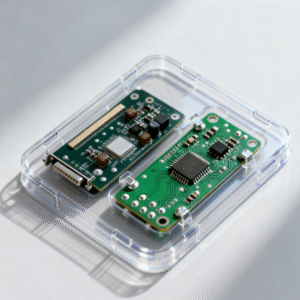
2 The Critical Role of ESD Protection in Electronic Packaging
2.1 The Hidden Danger of Electrostatic Discharge
Electrostatic Discharge (ESD) is a sudden flow of electricity between two charged objects, posing a severe threat to sensitive electronic components. While humans typically feel ESD at around 3,500 volts, modern microchips and circuits can be damaged by discharges as low as 5 volts. This damage can be:
Catastrophic: Immediate and complete failure of the component.
Latent: A partial degradation that weakens the component, causing premature failure in the field, which is often more costly and damaging to brand reputation.
2.2 Industry Standards and Requirements
International standards, such as ANSI/ESD S20.20, define the requirements for an Electrostatic Protected Area (EPA). Packaging materials within this scope must control static electricity effectively. Key performance metrics include:
Surface Resistance: Optimal range for dissipative materials is typically between 10^4 and 10^11 ohms/sq.
Charge Decay Time: The time for a charged voltage to reduce to a safe level, often required to be less than 2.0 seconds from 5000V.
2.3 The High Cost of Failure: Real-World Cases
The consequences of inadequate ESD packaging are severe and well-documented:
A major semiconductor manufacturer experienced a 40% rejection rate of microprocessors during testing due to ESD damage from non-compliant packaging. Switching to proper conductive carriers reduced rejections by over 60%.
A TFT-LCD module producer discovered that 0.36% of display failures were caused by ESD from packaging liners during manual handling, despite the materials initially testing “within spec.”
These cases demonstrate that ESD-related losses directly impact profitability, product quality, and customer trust.
3 The Superiority of Permanent Built-in ESD Technology
3.1 Limitations of Surface Coating Technology (Coating-Outside)
Surface-applied anti-static coatings are a temporary solution with significant drawbacks:
Limited Lifespan: The coating can be easily rubbed off or worn away through normal handling and shipping, leading to a rapid decline in performance.
Environmental Sensitivity: Their effectiveness is often highly dependent on ambient humidity, failing in dry conditions.
Inconsistent Coverage: Achieving a uniform, pinhole-free coating on complex, deep-drawn trays is challenging, creating weak spots in protection.
Contamination Risk: The coating can generate particulate debris, a critical concern in cleanroom environments for semiconductor packaging.
3.2 Advantages of Permanent Built-in ESD Technology
Permanent built-in ESD protection is achieved by incorporating conductive materials (e.g., carbon nanotubes, carbon fibers, or inherently static-dissipative polymers) directly into the plastic resin matrix. This creates a permanent, homogeneous conductive network throughout the entire material.Here also introducing the advantage:Permanent Built-In ESD Plastic Sheets | Superior to Coating
Key Advantages:
Permanent Performance: The ESD protection is integral to the material and cannot be worn off, ensuring consistent performance throughout the product’s entire lifecycle.
Humidity Independence: Effectiveness does not rely on atmospheric conditions, providing reliable protection in all environments.
Uniform & Comprehensive Protection: Every surface, including edges and deep corners, offers the same level of ESD safety.
High Cleanliness: No risk of flaking or outgassing, making it ideal for sensitive applications.
Lower Total Cost of Ownership (TCO): Eliminates the need for re-coating, testing, and replacement of failed packaging, offering better long-term value.
Table: Performance Comparison: Surface Coating vs. Built-in ESD
| Feature | Surface Coating | Permanent Built-in ESD |
|---|---|---|
| Lifespan | Temporary, degrades with use | Permanent, lasts product lifetime |
| ESD Consistency | Can be uneven | Homogeneous throughout the part |
| Humidity Dependency | High | None |
| Risk of Contamination | Yes, from coating wear | Very Low |
| Cleanroom Suitability | Limited | Excellent |
| Long-Term Cost | Higher (recurring) | Lower (one-time investment) |
4 Implementation and Future Outlook
4.1 Implementing Built-in ESD Solutions
For manufacturers transitioning to superior ESD packaging, suggest a structured approach:
Conduct an ESD Audit: Identify vulnerability points in your production and supply chain.
Select the Right Material: Choose a vacuum-formable plastic compound (e.g., PETG, ABS) with the appropriate type and level of permanent ESD properties for your application.
Optimize Thermoforming Parameters: Work with your packaging supplier to fine-tune heating, vacuum, and cooling cycles for the new material to ensure optimal part quality and ESD performance.
Establish Quality Control: Implement rigorous incoming and ongoing testing of packaging for surface resistance and decay time.
4.2 Future Trends
The future of ESD packaging is moving towards smarter and more sustainable solutions:
Advanced Nanomaterials: The use of single-wall carbon nanotubes (SWCNTs) allows for exceptional ESD performance at very low loading levels, preserving the material’s mechanical properties and clarity.
Sustainability: The development of recyclable and bio-based polymers with built-in ESD properties is gaining momentum, aligning with circular economy goals.
Smart Packaging: Integration of RFID tags and sensors into ESD packaging enables track-and-trace and monitoring of environmental conditions during shipping.
Conclusion and Recommendations
The evolution of electronic packaging demands a shift from unreliable surface coatings to integrated, permanent ESD protection. Vacuum thermoforming with built-in anti-static properties provides a robust, reliable, and economically viable solution that safeguards valuable electronics against electrostatic damage.
Key Recommendations:
Prioritize Permanent Solutions: For high-value or sensitive components, invest in packaging with permanent built-in ESD properties.
Partner with Experts: Collaborate with vacuum thermoforming suppliers who have proven expertise in ESD materials and processing.
Focus on Total Cost, Not Just Unit Price: Evaluate packaging based on Total Cost of Ownership, including failure rates, handling efficiency, and longevity.
By adopting permanent built-in ESD vacuum thermoforming, electronics manufacturers can significantly enhance product quality, reduce costly field failures, and strengthen their market reputation for reliability.
Nbetmexico… Hecho en Mexico? Good! They’ve got some cool localized games. Customer service was helpful when I had a question. I’ll be back: nbetmexico